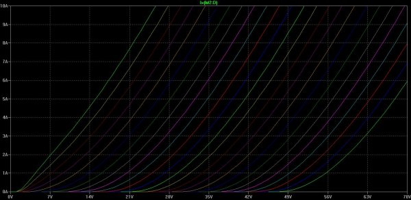
If I understand the design right, the answer is right in this graph:

Check on the left where the response is linear (flat line). At low input currents you basically have a tiny region which will not allow much swings around 2 volts. Push the input current way high and you get to the top graph where you now can have a healthy swing around 2 volt. Just like a class A design, you are having to bias the transistor with tons of idle current which goes to waste and needs to go some place. You also have pretty small voltage swings. Careful selection of FETs may provide a better center voltage but still, between the high input current and low voltage swings, making high power version of this will be tall mountain to climb.
Maybe a better picture would clarify


